Computer Architecture I @ ShanghaiTech University
Goals
- Install and set up Logisim Evolution, a digital logic simulator.
- Get familiar with the Logisim Evolution interface.
- Build and simulate basic combinational logic circuits.
- Build and simulate a simple sequential logic circuit.
Exercises
Download the Lab 5 starter files before you begin.
Exercise 0: Install Logisim Evolution
Logisim Evolution is an open-source digital logic designer and simulator, actively maintained on GitHub. We will use it to design and simulate circuits throughout this course.
The latest release is v4.1.0.
Ubuntu (amd64)
Download the
.debpackage (browser orcurl):Or via
curl:curl -L -O https://github.com/Heaticy/logisim-evolution/releases/download/v4.1.0/logisim-evolution_4.1.0_amd64.deb
Install it using
apt(automatically handles dependencies):sudo apt install ./logisim-evolution_4.1.0_amd64.deb
Launch Logisim Evolution from your application menu, or run:
logisim-evolution
macOS
Download the
.pkgpackage matching your chip, browser orcurl:Apple Silicon (M-series): https://github.com/Heaticy/logisim-evolution/releases/download/v4.1.0/logisim-evolution-4.1.0-aarch64.pkg
curl -L -O https://github.com/Heaticy/logisim-evolution/releases/download/v4.1.0/logisim-evolution-4.1.0-aarch64.pkgIntel (x86_64): https://github.com/Heaticy/logisim-evolution/releases/download/v4.1.0/logisim-evolution-4.1.0-x86_64.pkg
curl -L -O https://github.com/Heaticy/logisim-evolution/releases/download/v4.1.0/logisim-evolution-4.1.0-x86_64.pkg
Double-click the
.pkgfile to install.Launch Logisim Evolution from Applications, or run
logisim-evolutionin the terminal. If macOS blocks the app on first launch, go to System Settings → Privacy & Security and click Open Anyway.
Fallback: Any Platform (via Java JAR)
If none of the above installation methods work, you can run Logisim Evolution directly via Java.
- Download the
.jarfile: - Install Java 21:
- Ubuntu:
sudo apt install openjdk-21-jdk - macOS:
brew install openjdk@21
- Ubuntu:
- Launch Logisim Evolution:
java -jar logisim-evolution-4.1.0-all.jar
- For testing, place the
.jarfile in the same directory astest.shbefore running the test script.
Checkoff
- Show the TA that Logisim Evolution launches successfully on your machine.
Exercise 1: Hello World in Logisim
Once Logisim Evolution is running, you should see the welcome screen. In this part of the lab, we will create a simple AND gate circuit to get started quickly. Please pay attention to the zoom and grid functions located at the bottom left corner of the program, which will facilitate your wiring process during larger circuit designs.
Place an
ANDgate.
Start by clicking the
ANDgate button in the "Gates" folder. It will show a semi-transparentANDgate that follows your mouse pointer as you move it. Click once within the main schematic window to place anANDgate.Place two
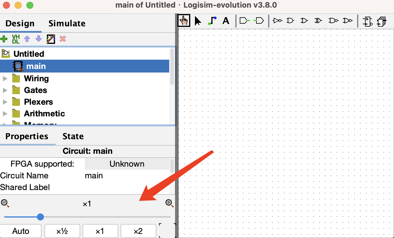
Input Pins.
Click the
Input Pinbutton in the toolbar at the top. Now, place two input pins somewhere to the left of yourANDgate.Place an
Output Pin.
Click the
Output Pinbutton in the toolbar at the top. Then place an output pin somewhere to the right of yourANDgate. Your schematic should look something like the figures above.Connect the pins with wires using the
Selecttool.
Click the
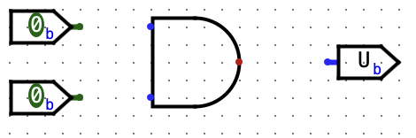
Selecttool button. Click and drag to connect the input pins to the left side of theANDgate. This will take several steps, as you can only draw vertical and horizontal wires. Just draw a wire horizontally, release the mouse button, then click and drag starting from the end of the wire to continue vertically. You can attach the wire to any pin on theANDgate on the left side. Repeat the same procedure to connect the output of theANDGate (right side) to the output pin. Double-click these three pins to name their labels. For this exercise, you should label the two input pins asAandB, and label the output pin asRESULT. These exact labels are important because the test vector loader matches signals by pin label. After completing these steps your schematic should look roughly like the figures above.Test your circuit with the
Poketool.
Click the
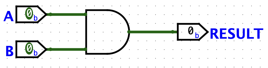
Poketool and try clicking on the input pins in your schematic. Observe what happens. Does this match with what you think anANDGate should do? Note that poking the wires themselves tells you the current value on that wire; this will be very useful later when you build more complex circuits.Save and run the test vector.
Save your circuit named as
ex1.circ. Before loading the test vector, make sure the two input pins are labeledAandB, and the output pin is labeledRESULT; otherwise,Simulate -> Test Vector...will not map the vector columns to the correct pins. Then load thetestvector_ex1.txtfile from thelab5_starterfolder. If everything goes well, you should see that all four test vectors passed.
Exercise 2: States
Let's implement a circuit that increments a value ad infinitum. The difference between this circuit and the circuits you've built for lab so far is that it will store this value in the state of a register.
ACTION ITEM:
The following steps will show you how to add registers to your circuit. Complete the steps and show the final circuit to your TA (remember to save!):
Open up the Exercise 2 schematic (
File -> Open -> ex2.circ) and go to the emptyAddMachinecircuit.Select the
Addersubcircuit from theArithmeticlibrary and place theAdderinto yourAddMachinesubcircuit.Select the register from the
Memoryfolder and place one register into your subcircuit. Below is an image diagraming the parts of a register.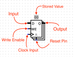
Connect a
clockto your register. You can find the clock circuit element in theWiringfolder in the circuit browser.Connect the output of the
Adderto the input of the register, and the output of the register to the input of theAdder.- You may get a "Incompatible widths" error when you try to connect components. This means that your wire is trying to connect two pins together with different bit widths. If you click on the
Adderwith theSelectiontool, you will notice that there is aData Bit Widthproperty in the bottom left field of the window. This value determines the number of bits each input and output theAdderhas. Change this field to8and the "Incompatible widths" error should be resolved.
- You may get a "Incompatible widths" error when you try to connect components. This means that your wire is trying to connect two pins together with different bit widths. If you click on the
Wire an 8-bit constant
1to the second input of theAdder. You can find theConstantcircuit element in theWiringlibrary.Connect the two output pins to your circuit so that you may monitor what comes out of the
Adderand the register. The output of theAddershould be connected toADD_OUTand the output of the register toREG_OUT.Select the
Comparatorsubcircuit from theArithmeticlibrary and place theComparatorinto yourAddMachinesubcircuit. The first input of theComparatorshould be connected toREG_OUT. Wire an 8-bit constant255to the second input of theComparator.Create an output pin at the right of the
Comparatorand name its label ashalt. Connect the second output of theComparatorto thehalt. It is used as a flag indicating the end of the simulation. Thus, by the end, your circuit should look like as follows: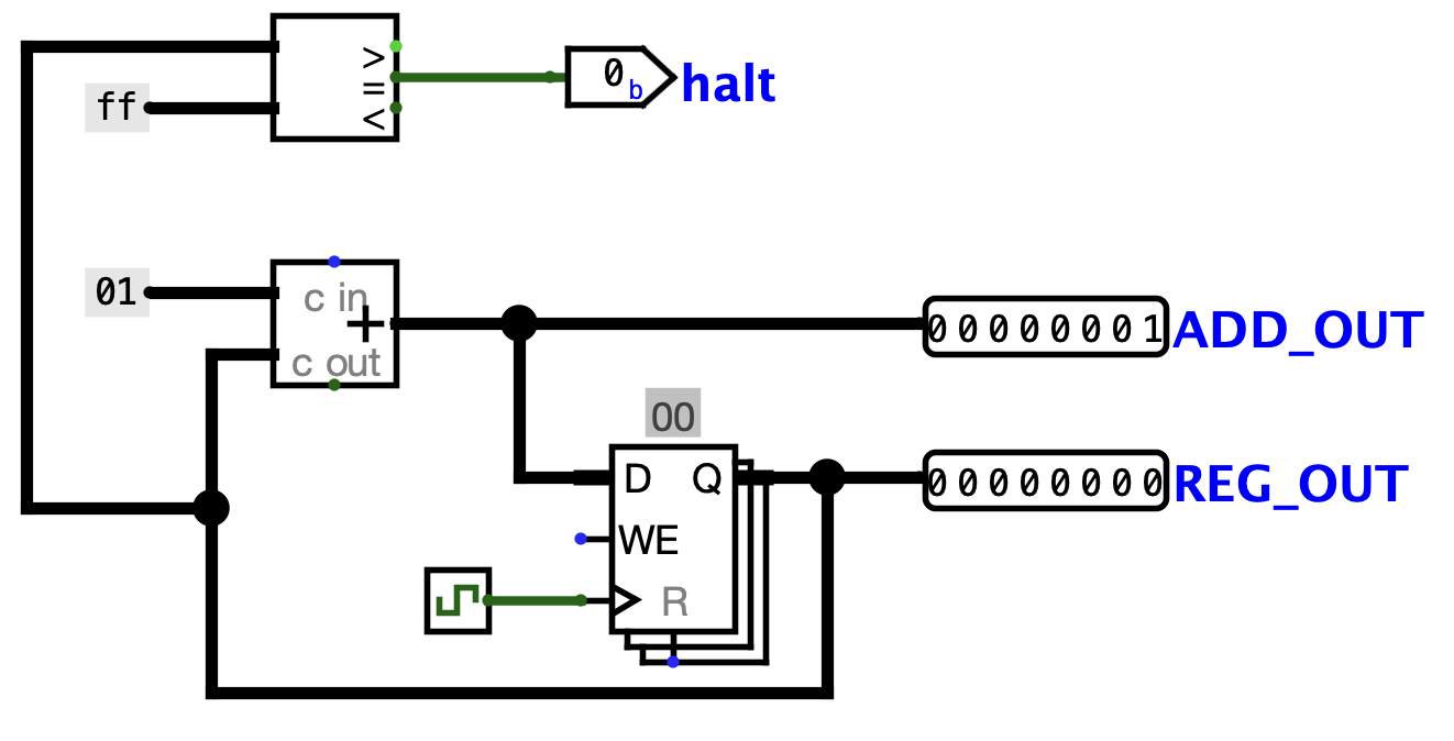
Now start running your circuit by going to
Simulate->Ticks Enabled(orCommand/Control + K). Your circuit should now be outputting a counter in binary form.If you want to run your circuit faster, you can change the tick frequency in
Simulate->Tick Frequency.
Checkoff
- Show your TA the completed
AddMachinecircuit and verify that it counts correctly. - Demonstrate that the circuit halts (the
haltoutput goes high) when the register reaches 255.
Part 2: Drawing circuit efficiently
Here are three Logisim features that should both save you a lot of time and make your circuits look much cleaner.
1. Splitters
Splitters allow you to take a multi-bit value and split it up into smaller parts, or (despite the name) combine multiple values that are one or more bits into a single value.
Here, we split the 4-bit binary number 0111 into 01 and 11, then recombine it with 10 into the final 6-bit number 100111:
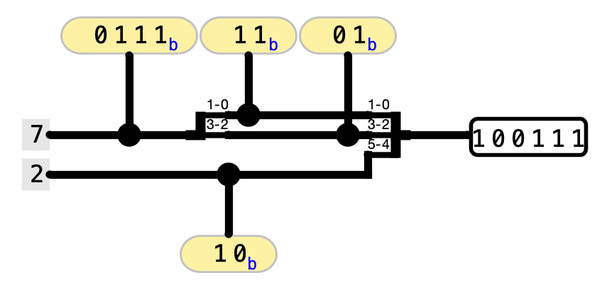
Click on a splitter to get its menu in the sidebar. This menu determine the number of arms on your splitter and how many bits should go on each arm. For the circuit above, the left splitter's menu looks like this:
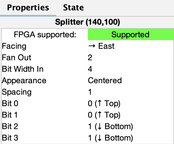
While the right splitter's menu looks like this:
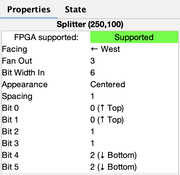
Notice that there's an option called facing. You can use this to rotate your splitter. Above, see that the splitter on the right faces West while the splitter on the left faces East.
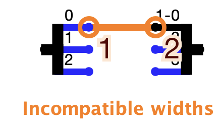
If you see an error wire that is orange, this means that your bit width in does not match your bit width out. Make sure that if you're connecting two components with a wire, you correctly set the bit width in that component's menu.
2. Tunnels
A tunnel allows you draw an "invisible wire" to bind two points together. Tunnels are grouped by case-sensitive labels give to a wire. They are used to connect wires as shown below:
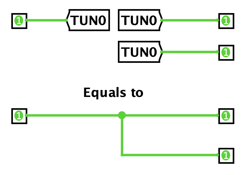
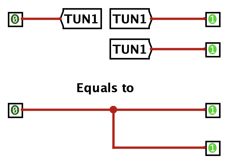
Some care should be taken as to which wires are connected with tunnels to which other wires, such as in this case:
We strongly recommend you use tunnels with Logisim, because they make your circuits much cleaner looking, and therefore easier to debug.
3. Extenders
When changing the width of a wire, you should use a bit extender for clarity. For example, consider the following implementation of extending an 8-bit wire into a 16-bit wire:
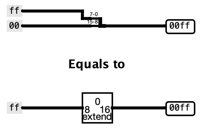
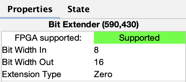
Compared to the splitter, the extender is easier to understand at a glance. This becomes especially helpful when working with complex circuits.
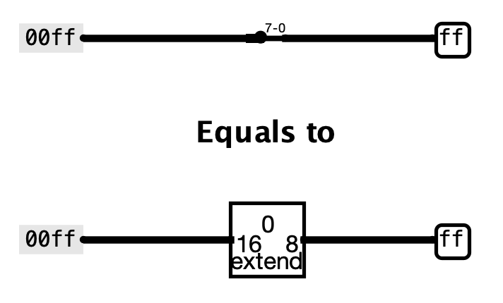
Additionally, consider the case of throwing out bits. Despite its name, an extender can also perform this operation:
Exercise 3: Practice with Advanced Features
In this part of the lab, we will construct a circuit that manipulates an 8-bit number.
ACTION ITEM:
Complete the following steps to create the splitter circuit, and show this to your TA (remember to save). When you've completed the circuit, answer the question in the checkoff session.
Open up the Exercise 3 schematic (
File->Open->ex3.circ) and go to the empty Split circuit.Go to the
Wiringfolder and select theSplittercircuit. This circuit will take a wire and split it into a set of wires of smaller width. Conversely, it can also take many sets of wires and combine them into one.Change the
Bit Width Inproperty (bus width) to8, andFan Outproperty to8. Connect the inputs to tunnels
Now, judge the number of '1's in the input whether odd. You can use
XORgates to eath bit of input and route the output toOUT1.Then, judge the number of '1's in the input whether greater than '0's. You can use
Bit Adder and ComparatorfromArithmeticto implement this circuit and route the output toOUT2.We need to append a parity bit to the most significant bit (MSB) of the input to ensure the output has an odd number of '1's. Without using Logisim's built-in parity gates, configure a splitter to merge the original input bits with the parity bit (placed before the MSB) and route the combined result to
OUT3.We consider the
OUT2is the sign bit of input, changing input into 2's complement format. Place another splitter with the proper properties to combine the sign bit and the 2's complement toOUT4.
Hint 1: An unsigned comparator is required in OUT2.
Hint 2: The parity bit can be obtained from OUT1 because when input has odd bit '1's, the parity bit will be 0, otherwise, the parity bit will be 1.
Hint 3: 2's complement transform is different according to sign bit.
Checkoff
- Show your
ex3.circto your TA and verify all four outputs (OUT1–OUT4) are correct. - When the output from
OUT4is negative and we want to compute its two's complement once more, what would the outcome be? Hint: In fact, this is a question about finding the two's complement of a two's complement. Share your findings with your TA.
Exercise 4: Rotate Right
With your knowledge and experience of splitters and multiplexers, you are ready to implement a non-trivial combinational logic block: rotr, which stands for "Rotate Right". The idea is that rotr A,B will "rotate" the bit pattern of input A to the right by B bits. So, if A were 0b1011010101110011 and B were 0b0101 (5 in decimal), the output of the block would be 0b1001110110101011. Notice that the rightmost 5 bits were rotated off the right end of the value and back onto the left end.
In other words, you need to design a combinational circuit for this equation: R = A >> B | A << (16 - B).
ACTION ITEM:
Implement a subcircuit named rotr with the following inputs. Show the final circuit to your TA (remember to save!).
A(16-bit), the 16-bit input to be rotatedB(4-bit), the rotation amount (why 4 bits?) You can find the starter subcircuit inex4.circ.
The output should be A rotated right by B bit positions, as outlined above. You are NOT allowed to use Logisim shifters in your solution. Complete your circuit by combinational logic (MUXes, constants, gates, adders, etc.)!. Logisim's built-in MUXes (find them under the Plexers menu) might be especialy helpful. Your solution shouldn't involve a clock or any clocked elements, like registers.
Hint 1: Before you start wiring, you should think very carefully about how you might decompose this problem into smaller ones and join them together. You should feel very free to use subcircuits when implementing rot4 and rot8 as well as rotr.
Hint 2: Think about the input bits of B and think about how to effectively use splitters! Can you do something with the binary form? Remember why binary is good for use in computers: a 1 is easy to represent as an ON signal, and a 0 is easy to represent as an OFF signal. Let's say we want to rotate 11 times. 11 is 1011 in binary, or 1*8 + 0*4 + 1*2 + 1*1. Can you use this to make a cleaner circuit? Making use of the rot*circuits we have provided is a good idea that will keep things clean!
Hint 3: Perhaps you also need to create other sub-circuits and call them in the rotr circuit. Please explore how to customize the appearance of your components! It's important to note that after designing their appearance, they also need to be saved immediately and their Appearance attribute should be changed to Custom.
Checkoff
- Show your TA your
rotrcircuit and verify that it works correctly for several different inputs.
Exercise 5: Running LED
From Exercise 4, we obtained a combinational circuits which can rotate the input with different values. In this part of lab, we will implement a version for sequential circuits. For each clock, the input will rotate with step of 1 and the rotated value will be input next time. For example, if input is 0b10000000 and we set the rotate step of 1. At clock 2, output is 0b01000000, at clock 3, output is 0b00100000...
ACTION ITEM:
Complete the following steps and show this completed circuit to your TA (remember to save!)
- Open up the Exercise 5 schematic (
File->Open->ex5.circ), you can use bulit-in components including Wiring, Gates, Plexers, Arithmetic and Memory now. - Using the
Registerto store the previous value, and then using arot1to rotate the value, the output isOUT_LED. - Using a
Multiplexerto set the initinal valueINITIAL_LEDofRegisterwhen reset signalRSTis 1. WhenRSTis 0, the input of Multiplexer will beOUT_LED.
For additional details about components, feel free to explore the Help-User's Guide
Checkoff
- Show your TA your
Running LEDcircuit and verify that it works correctly. - If we want the LED to stop after shifting exactly 8 times (remaining stationary until the next
RSTsignal), what changes should we make? Show your TA your revised circuit drawing or a new Logisim file containing the revised circuit.
Testing
Debugging circuits can be done in two ways. One method involves directly using the poke tool to alter component values and observe the output instantly. The second approach is to use the testing scripts provided by us via:
bash ./test.sh
The following TA(s) are responsible for this lab: Chaofan Li <lichf2025@shanghaitech.edu.cn>